Digital Electronic Circuit Design Using Basic Logic Gates Circuit Diagram The basic steps in modeling and analysis of a digital logic circuit are: 1. Open . Multisim. and create a "design" . 2. Draw a schematic diagram of the circuit (components and interconnections). 3. Design digital test patterns to b e applied to the circuit inputs to stimulate the circuit and Often, it's best to remove the potentially damaged chip from the build and test it independently from the other components in the electronics design. This article discusses a simple Arduino-based logic IC tester you can employ to find problems in your digital circuits. This image shows the completed build. BOM. Part/Quantity

Build and simulate circuits right in your browser. Design with our easy-to-use schematic editor. Analog & digital circuit simulations in seconds. Professional schematic PDFs, wiring diagrams, and plots. No installation required! Launch it instantly with one click. Launch CircuitLab or watch a quick demo video →
BreadBoardCircuits.com Circuit Diagram
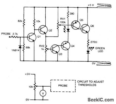
LED indicators to show the logic state; A circuit to drive the LEDs based on the probe input; When you touch the probe tip to a point in a digital circuit, the probe's internal circuitry compares the voltage at that point to a reference voltage, typically the supply voltage of the circuit under test.

Logisim is an educational tool for designing and simulating digital logic circuits. With its simple toolbar interface and simulation of circuits as they are built, it is simple enough to facilitate learning the most basic concepts related to logic circuits. allowing you to build up and test huge circuits; this step-by-step process just

How to Build a Simple Arduino Circuit Diagram
Input Test Circuit. This project will utilize an input test circuit consisting of several resistors and two switches. This test circuit will be used to test and demonstrate each logic gate. Below are both the schematic for the test circuit and picture of the breadboard. It will provide voltage outputs that represent logic levels 0 and 1. To best understand how to use this, let's create a test for the 4081 IC. This IC has four AND gates, so we will do a simple test that will try to turn on all the outputs for the AND gates. The image below shows the pinout and an overlay on the create test page so you can see which GPIO connect to which pins. For the probe to function correctly, the ground on the logic probe and the ground on the circuit under test must be connected. This is where the 0V ref pad comes into play. This pad gives you a place to connect your probe's ground to the ground of the circuit under test. Enclosure